


LUBIS EDA
LUBIS EDA Launches FormalOS: Infrastructure for Systematic, Scalable Formal Verification


The escalating complexity of artificial intelligence (AI) workloads, particularly those leveraging transformer-based models, is outpacing the capabilities of traditional transistor scaling. This has led to a fundamental shift in chip design philosophy: instead of adapting software to existing hardware, silicon is now being architected specifically for AI workloads. This “AI-first chip design” paradigm demands hardware that can handle massive parallelism and high-speed data movement within strict power and thermal limits.
3D-IC technology directly addresses these demands by vertically integrating multiple dies, such as high bandwidth memory (HBM) with logic, using through-silicon vias (TSVs). This vertical integration dramatically increases bandwidth (e.g., HBM3 and HBM3E stacks delivering 800 GB/s to over 1 TB/s per stack) and reduces latency, making it indispensable for advanced AI accelerators and high-performance computing.
However, this advancement comes with significant design challenges, such as:
These challenges underscore the need for advanced solutions that go beyond traditional EDA workflows, making AI-driven EDA not just beneficial, but essential. To address these challenges, AI is transforming EDA by embedding machine learning (ML) and reinforcement learning (RL) techniques directly into design tools. This enables automation and optimization across the design flow, tackling the immense complexity that human engineers can no longer manage alone. Let’s look at some key trends where 3D IC is being interwoven with AI.
Intelligent Design Space Exploration (DSE)
3D-IC architectures are exponentially complex, requiring designers to balance thousands or millions of interdependent variables (die partitioning, material stacks, floor planning, interconnect topology and power delivery), while optimizing for power, performance and area (PPA), reliability and cost. Manual iteration is slow and prone to suboptimal outcomes.
AI, through ML, RL, and surrogate modeling, drastically accelerates DSE. It allows teams to predict outcomes faster. AI models can quickly evaluate the impact of design choices.
AI can learn from previous iterations. Knowledge gained from past designs can be applied to new projects, reducing ramp-up time for next-generation architectures.
It can be used to uncover unconventional architectures. AI can identify optimal architectural plans that might be overlooked by traditional methods, delivering measurable improvements under multiple constraints.
AI is especially useful when it can augment human expertise. AI-powered copilots and agentic systems enable single design engineers to manage multiple complex blocks concurrently, significantly boosting productivity.
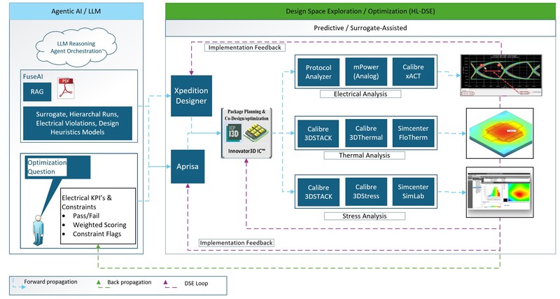
Figure 1: Agentic AI/LLM-driven, predictive/surrogate-assisted DSE loop across 3D IC electrical, thermal and stress workflows.
AI-driven DSE can be operationalized in real 3D-IC programs by combining an agentic AI/LLM layer with predictive/surrogate-assisted optimization and closing the loop across implementation plus three signoff workflows for electrical, thermal and stress analyses.
Figure 1 shows a closed-loop DSE workflow where an agentic AI/LLM layer interprets optimization questions and KPI constraints, then orchestrates implementation and integration. The flow connects to three multi-physics signoff workflows: electrical analysis producing artifacts such as S-parameters and eye diagrams, thermal analysis producing temperature maps and hotspot insight, and stress analysis producing stress/warpage and reliability-relevant results. Implementation feedback and KPI scoring drive iterative refinement toward an optimal solution.
In Figure 1, the agentic AI can sit “above” the implementation and multi-physics engines to make DSE practical at 3D-IC scale. The AI layer structures the optimization question into explicit electrical KPIs and constraints (pass/fail checks, weighted scoring, constraint flags), selects experiments, triggers tool runs and uses surrogate/predictive models to reduce the number of expensive full-fidelity iterations. Critically, the same DSE loop can span three coupled workflows—electrical, thermal and stress—so that improvements in one domain do not inadvertently create failures in another.
At 3D-IC scale, the limiting factor is often not the optimization concept, but the ability to securely orchestrate many heterogeneous tools, runs and artifacts across compute environments—this is where an MCP-based tool fabric fits.

Figure 2: MCP tool-fabric reference architecture for agentic 3D-IC design workflows.
Figure 2 illustrates an MCP (model context protocol) server–based “tool fabric” that sits between an agentic optimizer and the heterogeneous set of executables used in 3D-IC programs. Instead of point-to-point integrations, each capability is exposed as an MCP server with well-defined inputs/outputs and registered for discovery. An MCP host/bridge mediates secure tool invocation, environment setup, data movement and routing to local machines or HPC schedulers, while capturing logs, versions, parameters and produced artifacts. This architecture enables scalable, multi-tool experimentation and closed-loop optimization by normalizing results into KPI/evidence stores and making every run traceable and repeatable across teams, sites and tool chains.
Automated Power and Temperature-dependent Scaling
In 3D ICs, power and temperature are tightly coupled, creating a non-linear feedback loop: temperature changes leakage and power, which in turn shifts temperature. To converge quickly and accurately, teams need a scalable way to generate temperature-dependent power inputs for thermal analysis without repeatedly re-running full characterization at every corner.

Figure 3: AI-driven thermal-aware power modeling for design space exploration.
Temperature-dependent scaling flow (Figure 3) enables capturing baseline power at a single corner, building temperature-scaled libraries, mapping leakage vs. temperature at cell level, normalizing and generating multi-temperature power inputs, and closing the loop with 3D thermal analysis.
AI-Ready Chip Design Data
The efficacy of AI models hinges on the quality and accessibility of their training data. 3D-IC design generates petabytes of heterogeneous data (layout, electrical, thermal, mechanical, manufacturing, design exploration results, simulation outputs, characterization data, PDK information) often residing in disparate, siloed systems with inconsistent formats or noise.
Making this massive, multi-domain data ready for AI requires deliberate investment in design data and IP management. Curating, labeling and ensuring the quality and accessibility of data across the full design lifecycle is crucial. Scalable storage and compute platforms are also necessary as high-fidelity simulation outputs demand robust infrastructure.
Without these foundations, AI models risk learning spurious correlations, amplifying bias or producing untrustworthy results. This highlights the importance of a holistic approach to data management within the EDA ecosystem.
Addressing 3D-IC Challenges with Industrial-Grade AI
Industrial-grade AI is grounded in five foundational principles:
This industrial-grade AI approach augments human expertise, alleviates the burden of manual workflow management and enhances engineering throughput, ensuring that rigorous multi-physics validation scales with increasingly aggressive PPA requirements and time-to-market constraints.
Conclusion
As 3D-IC systems grow more complex and heterogeneous to meet the demands of the AI era, the combination of human expertise and AI-augmented design methodologies will be essential. Legacy chip designs are no longer sufficient to handle the massive parallelism and high-speed data movement required by modern AI workloads within strict power and thermal limits. Industrial-grade AI solutions empower design teams to navigate these challenges. By integrating intelligent design space exploration, automated power and thermal co-analysis and robust data management, AI is shaping the EDA ecosystem.
Read the extended white paper here: Three design imperatives to accelerate 3D IC design with AI
Author Bio:
Sudarshan Deo is a Software R&D Manager for 3D IC at Siemens Digital Industries Software in the Central Engineering Solutions Division. He holds an M.S. in Computer Science from California State University, Sacramento, and has expertise in implementing and integrating complex 3D IC workflows, including physical design, DFT, multi-physics, thermal, stress, SI, PI, and DC IR-drop analysis. He also contributes to initiatives in 3D UI and data management using IP lifecycle management and integrates advanced AI frameworks to optimize and enhance 3D IC workflows. He serves as a technical point of contact for divisions across Siemens Digital Industries Software. Previously, he was a Lead Software R&D Engineer at Cadence (flip-chip and 3D IC routing), a Senior Software R&D Engineer at Synopsys (3D IC SI and routing) and worked at Intel on RTL-to-GDSII flow automation, as well as post-silicon power and thermal validation software products.


